V3 size and arrangement

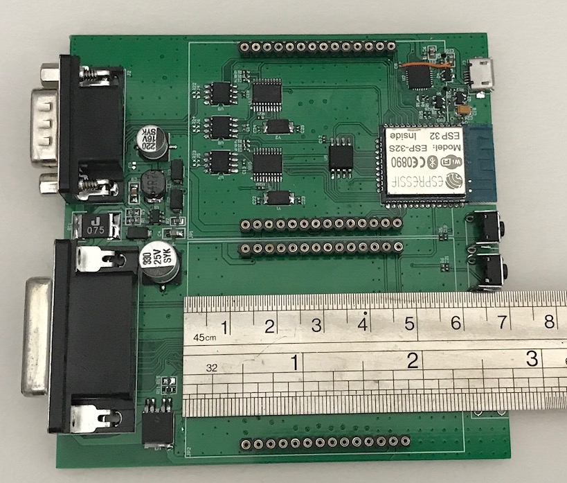
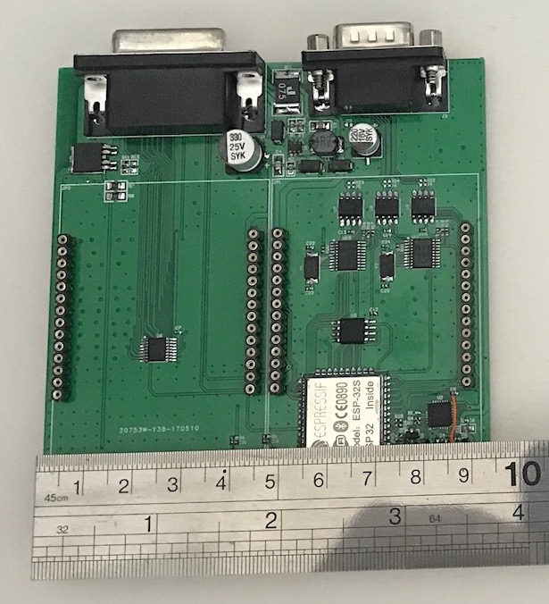
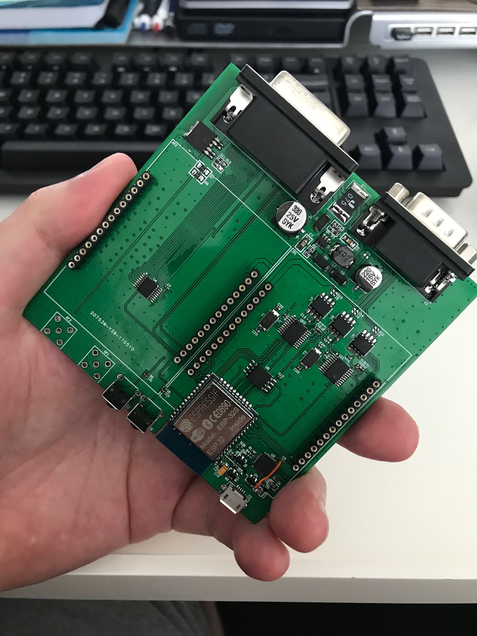
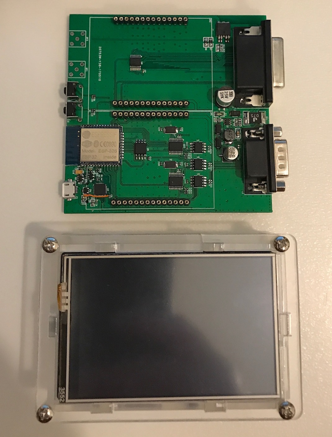
I've got the first OVMS v3 development board in my hands now. The components seem fine, and I'm finalizing the QC program that checks everything to make sure all is ok. 16MB flash with OTA capability, Wifi, Bluetooth, 3xCAN bus, lots of GPIO, switched 12V, power by USB/12V, SD card reader/writer, optional 2G/3G/4G modem (with GPS), two expansion slots, USB, and an external expansion connector - all look good. Both 3G and 4G development expansion boards are also being made now, and I should have those next week. But, having seen it and held it, I'm now having second thoughts about the layout. As you can see from the attached pictures, the expansion slots are each about 60mm x 45mm. Putting two of those on the board makes it about 9.5cm x 9.5cm square. Height will be similar (a little bit taller) than the current OVMS v2. This is a first draft run only, just to confirm the components, but as you can see there is quite a lot of blank space and traces for the two expansion slots. That, and the sheer number of connectors we have, dominate the board. Let's call this arrangement (A). There was an alternative arrangement that I considered a while back. That would be to have just one expansion slot, but use stackable connectors (so multiple boards could be piggybacked on each other). In that arrangement, the expansion slot could be either vertical or horizontal, with a vertical arrangement being close in size to the existing OVMS v2 (but the height would need to be much taller to accommodate the piggybacked expansion boards). Let's call this arrangement (B). It doesn't change the wiring. Just the size and arrangement of components on the board, as well as the box housing this all. (A) ends up with a 1" wider+taller box of about the same thickness, while (B) ends up with a box about the same width and height, but significantly thicker. To me, it seems that (A) is more automotive, and (B) more hobbyist. What do people think? In the meantime, on with development (now that at last I have a target in my hands). Mark

Personally, the v2 size is great because it is close to the same size as the electronic toll road device in cars that get exported second hand from Japan. What would be ideal for in car development is a USB port and SIM card slot accessible out the front with the LEDs. If v3 was similar front area, even if significantly longer, that would still work! That's just what fits my personal need. More generally to make a more reliable product: expansion boards need to be mechanically latched. I have used brass threaded inserts soldered onto the main board. Use a low strength thread glue on the screws and they only come apart with a screwdriver. In other news there is potential for a bunch (20+) Leafs that need units in a relatively short timeframe. Are V3's likely to be going soon, or would v2's be safer? The porting to ARM is going to need a bit of testing correct? Edward
On 19/05/2017, at 6:23 PM, Mark Webb-Johnson wrote:
I've got the first OVMS v3 development board in my hands now. The components seem fine, and I'm finalizing the QC program that checks everything to make sure all is ok. 16MB flash with OTA capability, Wifi, Bluetooth, 3xCAN bus, lots of GPIO, switched 12V, power by USB/12V, SD card reader/writer, optional 2G/3G/4G modem (with GPS), two expansion slots, USB, and an external expansion connector - all look good.
Both 3G and 4G development expansion boards are also being made now, and I should have those next week.
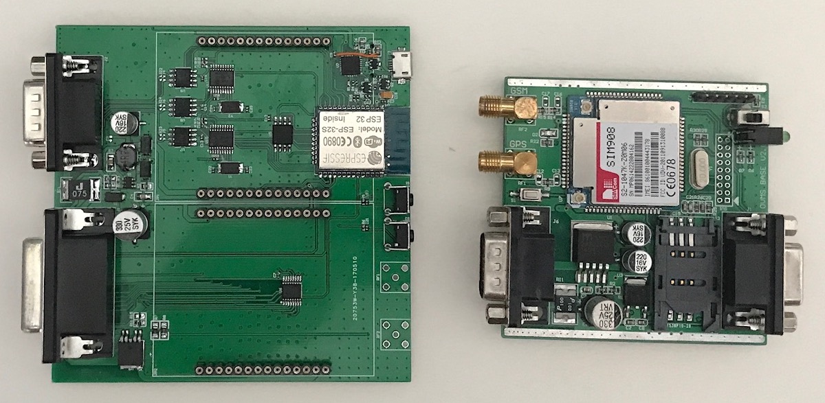
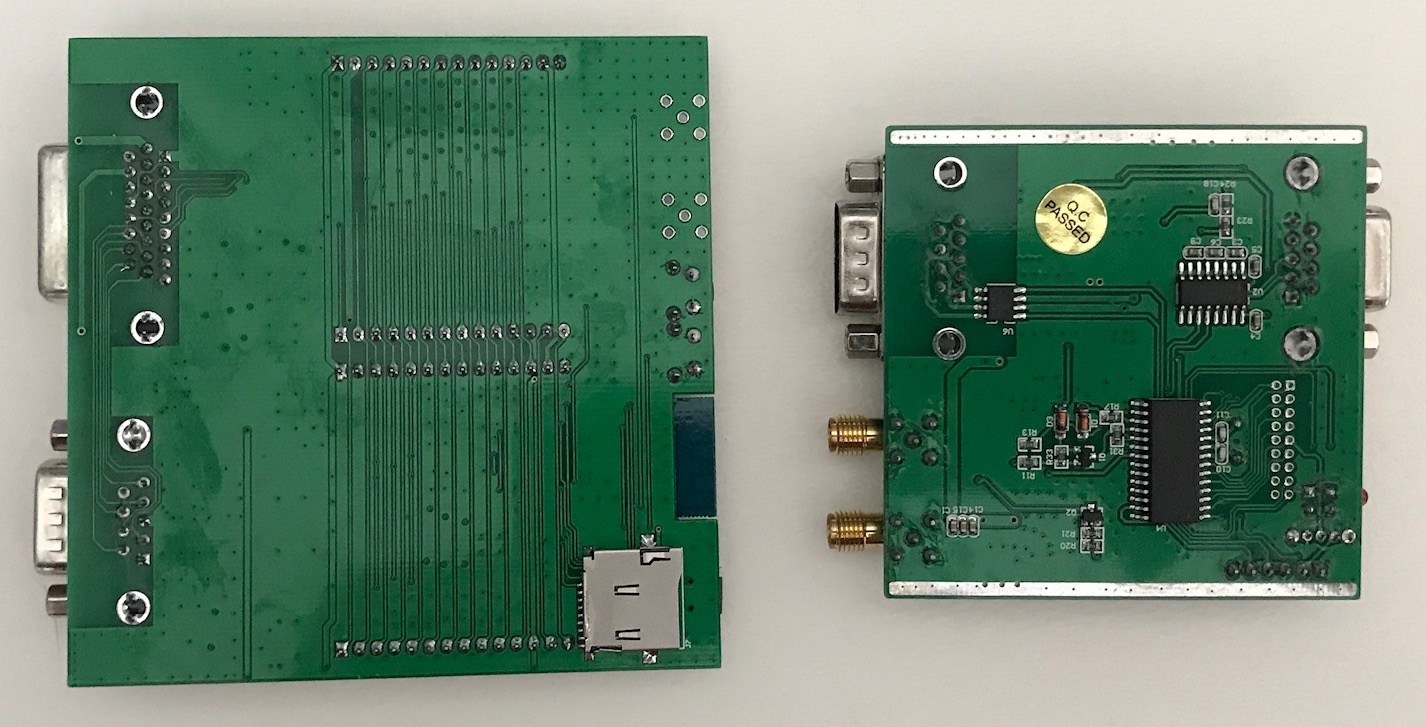
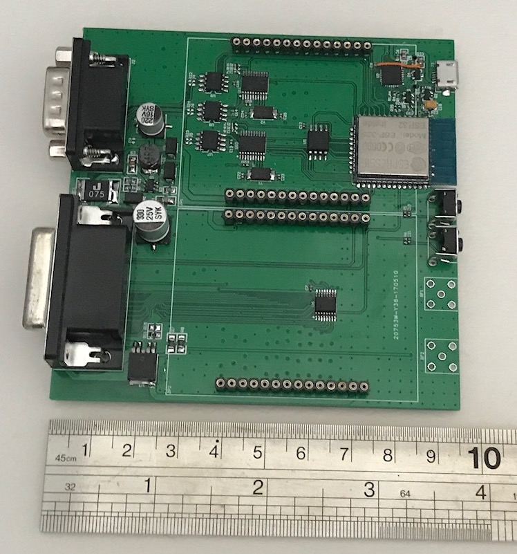
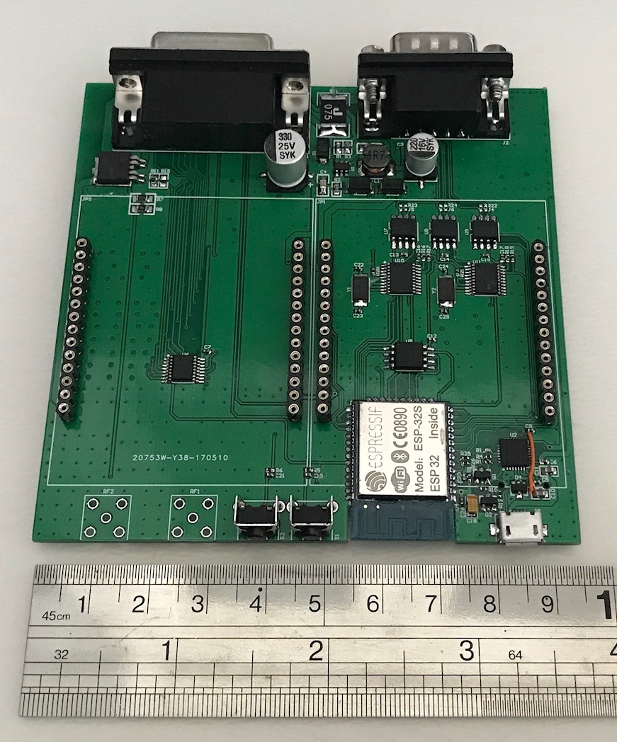
But, having seen it and held it, I'm now having second thoughts about the layout. As you can see from the attached pictures, the expansion slots are each about 60mm x 45mm. Putting two of those on the board makes it about 9.5cm x 9.5cm square. Height will be similar (a little bit taller) than the current OVMS v2. This is a first draft run only, just to confirm the components, but as you can see there is quite a lot of blank space and traces for the two expansion slots. That, and the sheer number of connectors we have, dominate the board. Let's call this arrangement (A).
There was an alternative arrangement that I considered a while back. That would be to have just one expansion slot, but use stackable connectors (so multiple boards could be piggybacked on each other). In that arrangement, the expansion slot could be either vertical or horizontal, with a vertical arrangement being close in size to the existing OVMS v2 (but the height would need to be much taller to accommodate the piggybacked expansion boards). Let's call this arrangement (B).
It doesn't change the wiring. Just the size and arrangement of components on the board, as well as the box housing this all. (A) ends up with a 1" wider+taller box of about the same thickness, while (B) ends up with a box about the same width and height, but significantly thicker. To me, it seems that (A) is more automotive, and (B) more hobbyist.
What do people think?
In the meantime, on with development (now that at last I have a target in my hands).
Mark
<image1.jpeg>
<image2.jpeg>
<image3.jpeg>
<image4.jpeg>
<image5.jpeg>
<image6.jpeg>
<image7.jpeg> _______________________________________________ OvmsDev mailing list OvmsDev@lists.teslaclub.hk http://lists.teslaclub.hk/mailman/listinfo/ovmsdev
Personally, the v2 size is great because it is close to the same size as the electronic toll road device in cars that get exported second hand from Japan.
Even if it was thicker? OVMS v2 is approximately 73mm x 73mm x 23mm. Making room for two stackable boards would probably increase it to 73mm x 73mm x 43mm.
What would be ideal for in car development is a USB port and SIM card slot accessible out the front with the LEDs.
USB port is reachable from outside. It is on the topside of the board (next to the ESP32 module) in the pictures I sent. SIM card slot accessible from outside is not so easy. Most of the trays around here are all top-down attached. A slide in tray may not be so easy to find. Why do we need to change SIM card so much? Or do you mean SD CARD slot? The SD card is on the bottom of the board, under the USB connector and we are arranging for it to be reachable from outside.
More generally to make a more reliable product: expansion boards need to be mechanically latched. I have used brass threaded inserts soldered onto the main board. Use a low strength thread glue on the screws and they only come apart with a screwdriver.
Really? Even with two rows of 14pin SIP socket? That is pretty robust. I can ask what the manufacturer recommends.
In other news there is potential for a bunch (20+) Leafs that need units in a relatively short timeframe. Are V3's likely to be going soon, or would v2's be safer? The porting to ARM is going to need a bit of testing correct?
20 would be hard for OVMS v2. MOQ if 100 for batches machine-soldered. I just want to get the board finalised then will commit and release what framework code I have. Everything needs to be ported over, but I’m really just concentrating on the framework side (in particular communications, SD CARD and OTA updates - so we can update firmware). Regards, Mark.
On 19 May 2017, at 3:56 PM, Edward Cheeseman <cheesemanedward@gmail.com> wrote:
Personally, the v2 size is great because it is close to the same size as the electronic toll road device in cars that get exported second hand from Japan.
What would be ideal for in car development is a USB port and SIM card slot accessible out the front with the LEDs.
If v3 was similar front area, even if significantly longer, that would still work!
That's just what fits my personal need.
More generally to make a more reliable product: expansion boards need to be mechanically latched. I have used brass threaded inserts soldered onto the main board. Use a low strength thread glue on the screws and they only come apart with a screwdriver.
In other news there is potential for a bunch (20+) Leafs that need units in a relatively short timeframe. Are V3's likely to be going soon, or would v2's be safer? The porting to ARM is going to need a bit of testing correct?
Edward
On 19/05/2017, at 6:23 PM, Mark Webb-Johnson wrote:
I've got the first OVMS v3 development board in my hands now. The components seem fine, and I'm finalizing the QC program that checks everything to make sure all is ok. 16MB flash with OTA capability, Wifi, Bluetooth, 3xCAN bus, lots of GPIO, switched 12V, power by USB/12V, SD card reader/writer, optional 2G/3G/4G modem (with GPS), two expansion slots, USB, and an external expansion connector - all look good.
Both 3G and 4G development expansion boards are also being made now, and I should have those next week.
But, having seen it and held it, I'm now having second thoughts about the layout. As you can see from the attached pictures, the expansion slots are each about 60mm x 45mm. Putting two of those on the board makes it about 9.5cm x 9.5cm square. Height will be similar (a little bit taller) than the current OVMS v2. This is a first draft run only, just to confirm the components, but as you can see there is quite a lot of blank space and traces for the two expansion slots. That, and the sheer number of connectors we have, dominate the board. Let's call this arrangement (A).
There was an alternative arrangement that I considered a while back. That would be to have just one expansion slot, but use stackable connectors (so multiple boards could be piggybacked on each other). In that arrangement, the expansion slot could be either vertical or horizontal, with a vertical arrangement being close in size to the existing OVMS v2 (but the height would need to be much taller to accommodate the piggybacked expansion boards). Let's call this arrangement (B).
It doesn't change the wiring. Just the size and arrangement of components on the board, as well as the box housing this all. (A) ends up with a 1" wider+taller box of about the same thickness, while (B) ends up with a box about the same width and height, but significantly thicker. To me, it seems that (A) is more automotive, and (B) more hobbyist.
What do people think?
In the meantime, on with development (now that at last I have a target in my hands).
Mark
<image1.jpeg>
<image2.jpeg>
<image3.jpeg>
<image4.jpeg>
<image5.jpeg>
<image6.jpeg>
<image7.jpeg> _______________________________________________ OvmsDev mailing list OvmsDev@lists.teslaclub.hk http://lists.teslaclub.hk/mailman/listinfo/ovmsdev
OvmsDev mailing list OvmsDev@lists.teslaclub.hk http://lists.teslaclub.hk/mailman/listinfo/ovmsdev

In other news there is potential for a bunch (20+) Leafs that need units in a relatively short timeframe. Are V3's likely to be going soon, or would v2's be safer? The porting to ARM is going to need a bit of testing correct?
20 would be hard for OVMS v2. MOQ if 100 for batches machine-soldered.
It would be no problem to find buyers for another 20-30 units for the Twizy in my BulitinBoard. https://www.twizy.forum.de <https://www.twizy.forum.de/> Posts from users looking for used OVMS are quite common since the news got out that V2.5 was out of stock. Even when V3 would be finished, I still see a purpose for the V2.5 , since it would be smaller (Fits in the glovebox of the twizy). Maybe V2.5 and V3 can coexist and you chose the one that fits to your needs? Regards Frank
Ahhhrrrgggg! Made a mistake with the link!! www.twizy-forum.de <http://www.twizy-forum.de/> the other link will send you to a squatter site. Please do not click this one ;-)
Am 19.05.2017 um 13:03 schrieb Frank Demes <frank.demes@gmx.de>:
In other news there is potential for a bunch (20+) Leafs that need units in a relatively short timeframe. Are V3's likely to be going soon, or would v2's be safer? The porting to ARM is going to need a bit of testing correct?
20 would be hard for OVMS v2. MOQ if 100 for batches machine-soldered.
It would be no problem to find buyers for another 20-30 units for the Twizy in my BulitinBoard. https://www.twizy.forum.de <https://www.twizy.forum.de/>
Posts from users looking for used OVMS are quite common since the news got out that V2.5 was out of stock.
Even when V3 would be finished, I still see a purpose for the V2.5 , since it would be smaller (Fits in the glovebox of the twizy).
Maybe V2.5 and V3 can coexist and you chose the one that fits to your needs?
Regards Frank
_______________________________________________ OvmsDev mailing list OvmsDev@lists.teslaclub.hk http://lists.teslaclub.hk/mailman/listinfo/ovmsdev
On 19/05/2017, at 11:03 PM, Frank Demes wrote:
Posts from users looking for used OVMS are quite common since the news got out that V2.5 was out of stock.
Even when V3 would be finished, I still see a purpose for the V2.5 , since it would be smaller (Fits in the glovebox of the twizy).
Maybe V2.5 and V3 can coexist and you chose the one that fits to your needs?
The immediate problem with v2.5 is the 2g networks getting turned off in the next few years. The local interest for 20 is for a fleet that can afford to upgrade later when required. Cars may even be replaced before that happens. Personally I can't see me giving up my leaf any time soon, and I'm looking forward to two can interfaces, so I can track odometer and SOC and get some real efficiency data. The fleet cars are most interested in GPS and SOC, which v2.5 is fine as is.
Well, I don’t mind doing another production run of v2 SIM808 modules, but the minimum quantity is 100. Given the capabilities of the two platforms, I think people will choose v3 for (a) features, (b) expandability, and (c) future-proof modem module swap. The last batch I had built was 100. The first 50 went in days. the last 50 took two months. Things really seemed to slow down at the end. Maybe you guys ask around and see what sort of interest there is? Regards, Mark.
On 19 May 2017, at 7:36 PM, Edward Cheeseman <cheesemanedward@gmail.com> wrote:
On 19/05/2017, at 11:03 PM, Frank Demes wrote:
Posts from users looking for used OVMS are quite common since the news got out that V2.5 was out of stock.
Even when V3 would be finished, I still see a purpose for the V2.5 , since it would be smaller (Fits in the glovebox of the twizy).
Maybe V2.5 and V3 can coexist and you chose the one that fits to your needs?
The immediate problem with v2.5 is the 2g networks getting turned off in the next few years. The local interest for 20 is for a fleet that can afford to upgrade later when required. Cars may even be replaced before that happens. Personally I can't see me giving up my leaf any time soon, and I'm looking forward to two can interfaces, so I can track odometer and SOC and get some real efficiency data. The fleet cars are most interested in GPS and SOC, which v2.5 is fine as is. _______________________________________________ OvmsDev mailing list OvmsDev@lists.teslaclub.hk http://lists.teslaclub.hk/mailman/listinfo/ovmsdev
On 19/05/2017, at 10:48 PM, Mark Webb-Johnson wrote:
Personally, the v2 size is great
Even if it was thicker? OVMS v2 is approximately 73mm x 73mm x 23mm. Making room for two stackable boards would probably increase it to 73mm x 73mm x 43mm.
The toll road things are thinner than 23mm, but there is height room to grow into. I've lost track of why two expansion boards are needed but I think it was for GPIO expandability. Having the cell modem changeable seems sensible given the international fragmented cell frequencies. Given that, I can't see how to fit them in without going to the height you have said. Simple answer: I like your stacked version better. The wider version wouldn't be a deal breaker though. Let's see what others think.
SIM card slot accessible from outside is not so easy. Most of the trays around here are all top-down attached. A slide in tray may not be so easy to find. Why do we need to change SIM card so much? Only for development - I think I have hit an issue with a local cell provider and the SIM808 module not being able to reply to SMS. If it had been easily accessible I would have swapped a few SIM cards in to try. But no, it's not a real product requirement so disregard.
More generally to make a more reliable product: expansion boards need to be mechanically latched.
Really? Even with two rows of 14pin SIP socket? That is pretty robust. I can ask what the manufacturer recommends. Automotive is a high vibration environment, and friction alone can work loose. Maybe a recommendation to use a bit of hot glue, or cram some foam between the expansion boards and case would be more than sufficient. So again, probably don't bother as there are simple ways of fixing it if it ever becomes an issue.
Edward
Perhaps I can ask for two holes on each of the expansion slots (and lined up with holes on the expansion cards). Then we could use simple stand-offs if required. I’ll add it to the list of things to ask the factory what they think. Regards, Mark
On 19 May 2017, at 8:00 PM, Edward Cheeseman <cheesemanedward@gmail.com> wrote:
On 19/05/2017, at 10:48 PM, Mark Webb-Johnson wrote:
Really? Even with two rows of 14pin SIP socket? That is pretty robust. I can ask what the manufacturer recommends. Automotive is a high vibration environment, and friction alone can work loose. Maybe a recommendation to use a bit of hot glue, or cram some foam between the expansion boards and case would be more than sufficient. So again, probably don't bother as there are simple ways of fixing it if it ever becomes an issue.
Edward _______________________________________________ OvmsDev mailing list OvmsDev@lists.teslaclub.hk http://lists.teslaclub.hk/mailman/listinfo/ovmsdev

Is there provisioning in the v.3 hardware for switching off? I have killed numerous aux. batteries with my v.2 units and would appreciate possibility for the v.3 to switch itself off, and I mean totally off, not just the processor, but all leds, converters, etc. Nikolay On Friday, May 19, 2017, 9:58:07 AM GMT+2, Edward Cheeseman <cheesemanedward@gmail.com> wrote:Personally, the v2 size is great because it is close to the same size as the electronic toll road device in cars that get exported second hand from Japan. What would be ideal for in car development is a USB port and SIM card slot accessible out the front with the LEDs. If v3 was similar front area, even if significantly longer, that would still work! That's just what fits my personal need. More generally to make a more reliable product: expansion boards need to be mechanically latched. I have used brass threaded inserts soldered onto the main board. Use a low strength thread glue on the screws and they only come apart with a screwdriver. In other news there is potential for a bunch (20+) Leafs that need units in a relatively short timeframe. Are V3's likely to be going soon, or would v2's be safer? The porting to ARM is going to need a bit of testing correct? Edward
On 19/05/2017, at 6:23 PM, Mark Webb-Johnson wrote:
I've got the first OVMS v3 development board in my hands now. The components seem fine, and I'm finalizing the QC program that checks everything to make sure all is ok. 16MB flash with OTA capability, Wifi, Bluetooth, 3xCAN bus, lots of GPIO, switched 12V, power by USB/12V, SD card reader/writer, optional 2G/3G/4G modem (with GPS), two expansion slots, USB, and an external expansion connector - all look good.
Both 3G and 4G development expansion boards are also being made now, and I should have those next week.
But, having seen it and held it, I'm now having second thoughts about the layout. As you can see from the attached pictures, the expansion slots are each about 60mm x 45mm. Putting two of those on the board makes it about 9.5cm x 9.5cm square. Height will be similar (a little bit taller) than the current OVMS v2. This is a first draft run only, just to confirm the components, but as you can see there is quite a lot of blank space and traces for the two expansion slots. That, and the sheer number of connectors we have, dominate the board. Let's call this arrangement (A).
There was an alternative arrangement that I considered a while back. That would be to have just one expansion slot, but use stackable connectors (so multiple boards could be piggybacked on each other). In that arrangement, the expansion slot could be either vertical or horizontal, with a vertical arrangement being close in size to the existing OVMS v2 (but the height would need to be much taller to accommodate the piggybacked expansion boards). Let's call this arrangement (B).
It doesn't change the wiring. Just the size and arrangement of components on the board, as well as the box housing this all. (A) ends up with a 1" wider+taller box of about the same thickness, while (B) ends up with a box about the same width and height, but significantly thicker. To me, it seems that (A) is more automotive, and (B) more hobbyist.
What do people think?
In the meantime, on with development (now that at last I have a target in my hands).
Mark
<image1.jpeg>
<image2.jpeg>
<image3.jpeg>
<image4.jpeg>
<image5.jpeg>
<image6.jpeg>
<image7.jpeg> _______________________________________________ OvmsDev mailing list OvmsDev@lists.teslaclub.hk http://lists.teslaclub.hk/mailman/listinfo/ovmsdev
OvmsDev mailing list OvmsDev@lists.teslaclub.hk http://lists.teslaclub.hk/mailman/listinfo/ovmsdev
Not completely off (at present). We can turn off the modem, and any external 12V loads. We can shut down the SPI CAN bus. Then, we can power down the main MCU. I think the resulting vampire drain should be tiny. By far the greatest drain comes from the modem. We’re also using a switching power supply (not a simple LM like before), for the best efficiency that we can get. I’ll do some test measurements, when I have some time in the next day or two. It is an important goal to be able to get the power down as minimal as possible. A latching power supply is possible - just uses up another I/O pin. Regards, Mark. P.S. I feel for Elon Musk when he recently said that Model T will have no 12V, but a more sensible power supply (presumably 5V or 3.3V). Every module in the car has to step down 12V -> 3.3V, and that wastes a lot of power. Even switching mode is not 100% efficient and introduces more noise in the power lines.
On 19 May 2017, at 7:33 PM, Nikolay Shishkov <nshishkov@yahoo.com> wrote:
Is there provisioning in the v.3 hardware for switching off? I have killed numerous aux. batteries with my v.2 units and would appreciate possibility for the v.3 to switch itself off, and I mean totally off, not just the processor, but all leds, converters, etc. Nikolay
On Friday, May 19, 2017, 9:58:07 AM GMT+2, Edward Cheeseman <cheesemanedward@gmail.com> wrote: Personally, the v2 size is great because it is close to the same size as the electronic toll road device in cars that get exported second hand from Japan.
What would be ideal for in car development is a USB port and SIM card slot accessible out the front with the LEDs.
If v3 was similar front area, even if significantly longer, that would still work!
That's just what fits my personal need.
More generally to make a more reliable product: expansion boards need to be mechanically latched. I have used brass threaded inserts soldered onto the main board. Use a low strength thread glue on the screws and they only come apart with a screwdriver.
In other news there is potential for a bunch (20+) Leafs that need units in a relatively short timeframe. Are V3's likely to be going soon, or would v2's be safer? The porting to ARM is going to need a bit of testing correct?
Edward
On 19/05/2017, at 6:23 PM, Mark Webb-Johnson wrote:
I've got the first OVMS v3 development board in my hands now. The components seem fine, and I'm finalizing the QC program that checks everything to make sure all is ok. 16MB flash with OTA capability, Wifi, Bluetooth, 3xCAN bus, lots of GPIO, switched 12V, power by USB/12V, SD card reader/writer, optional 2G/3G/4G modem (with GPS), two expansion slots, USB, and an external expansion connector - all look good.
Both 3G and 4G development expansion boards are also being made now, and I should have those next week.
But, having seen it and held it, I'm now having second thoughts about the layout. As you can see from the attached pictures, the expansion slots are each about 60mm x 45mm. Putting two of those on the board makes it about 9.5cm x 9.5cm square. Height will be similar (a little bit taller) than the current OVMS v2. This is a first draft run only, just to confirm the components, but as you can see there is quite a lot of blank space and traces for the two expansion slots. That, and the sheer number of connectors we have, dominate the board. Let's call this arrangement (A).
There was an alternative arrangement that I considered a while back. That would be to have just one expansion slot, but use stackable connectors (so multiple boards could be piggybacked on each other). In that arrangement, the expansion slot could be either vertical or horizontal, with a vertical arrangement being close in size to the existing OVMS v2 (but the height would need to be much taller to accommodate the piggybacked expansion boards). Let's call this arrangement (B).
It doesn't change the wiring. Just the size and arrangement of components on the board, as well as the box housing this all. (A) ends up with a 1" wider+taller box of about the same thickness, while (B) ends up with a box about the same width and height, but significantly thicker. To me, it seems that (A) is more automotive, and (B) more hobbyist.
What do people think?
In the meantime, on with development (now that at last I have a target in my hands).
Mark
<image1.jpeg>
<image2.jpeg>
<image3.jpeg>
<image4.jpeg>
<image5.jpeg>
<image6.jpeg>
<image7.jpeg> _______________________________________________ OvmsDev mailing list OvmsDev@lists.teslaclub.hk <mailto:OvmsDev@lists.teslaclub.hk> http://lists.teslaclub.hk/mailman/listinfo/ovmsdev <http://lists.teslaclub.hk/mailman/listinfo/ovmsdev>
_______________________________________________ OvmsDev mailing list OvmsDev@lists.teslaclub.hk <mailto:OvmsDev@lists.teslaclub.hk> http://lists.teslaclub.hk/mailman/listinfo/ovmsdev <http://lists.teslaclub.hk/mailman/listinfo/ovmsdev> _______________________________________________ OvmsDev mailing list OvmsDev@lists.teslaclub.hk http://lists.teslaclub.hk/mailman/listinfo/ovmsdev

That looks great :)
From a first test (A) should still fit in the Twizy glove box, so should fit in other mounting places as well.
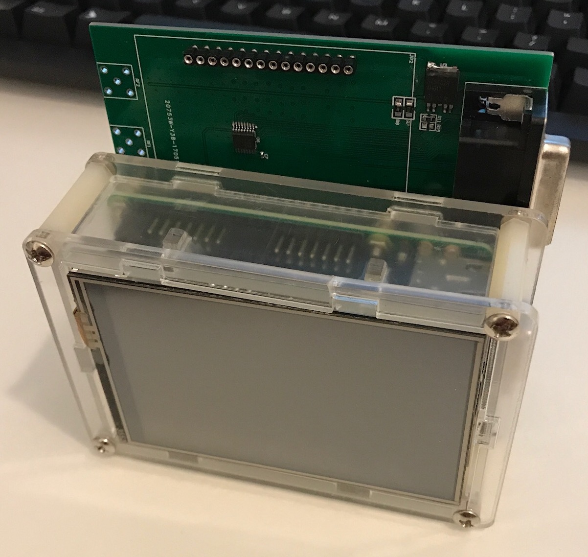
As mentioned earlier I think a touch screen would make a nice addon, and (A) seems to be better for mounting a large display directly to the board. That should still make a nice & handy box. I think (B) would become very clunky with a large display. So I'm tending towards (A). Regards, Michael Am 19.05.2017 um 08:23 schrieb Mark Webb-Johnson:
But, having seen it and held it, I'm now having second thoughts about the layout. As you can see from the attached pictures, the expansion slots are each about 60mm x 45mm. Putting two of those on the board makes it about 9.5cm x 9.5cm square. Height will be similar (a little bit taller) than the current OVMS v2. This is a first draft run only, just to confirm the components, but as you can see there is quite a lot of blank space and traces for the two expansion slots. That, and the sheer number of connectors we have, dominate the board. Let's call this arrangement (A).
There was an alternative arrangement that I considered a while back. That would be to have just one expansion slot, but use stackable connectors (so multiple boards could be piggybacked on each other). In that arrangement, the expansion slot could be either vertical or horizontal, with a vertical arrangement being close in size to the existing OVMS v2 (but the height would need to be much taller to accommodate the piggybacked expansion boards). Let's call this arrangement (B).
It doesn't change the wiring. Just the size and arrangement of components on the board, as well as the box housing this all. (A) ends up with a 1" wider+taller box of about the same thickness, while (B) ends up with a box about the same width and height, but significantly thicker. To me, it seems that (A) is more automotive, and (B) more hobbyist.
What do people think?
-- Michael Balzer * Helkenberger Weg 9 * D-58256 Ennepetal Fon 02333 / 833 5735 * Handy 0176 / 206 989 26
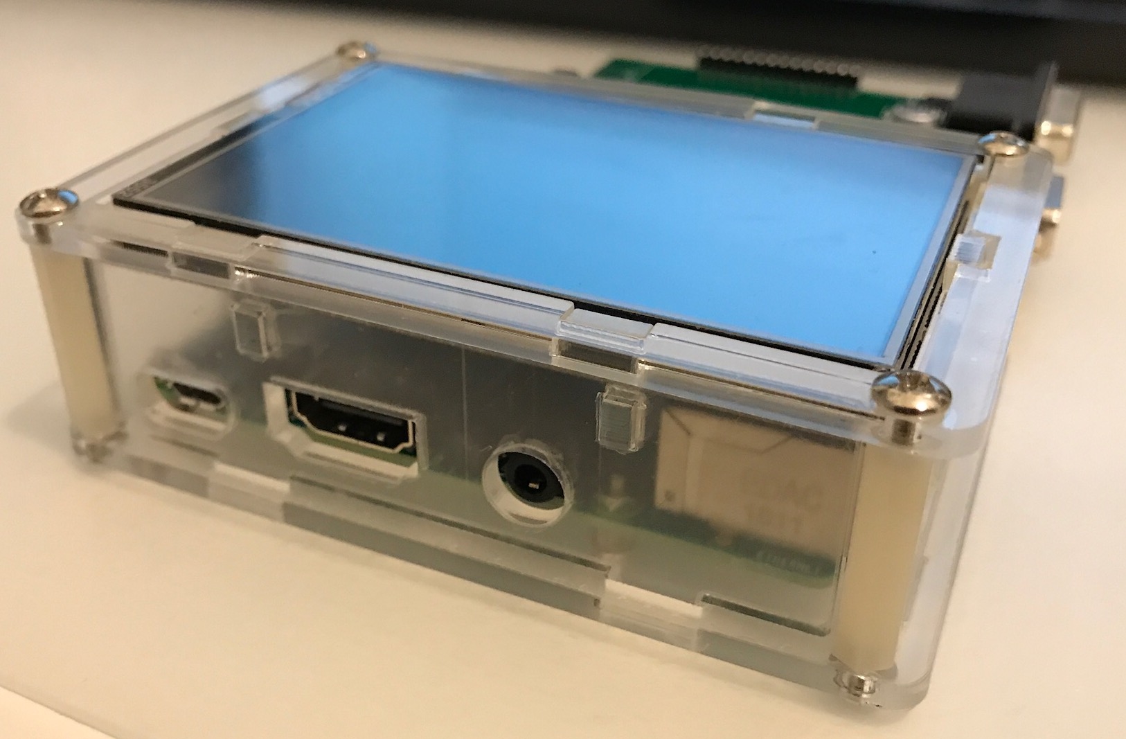
I see what you are saying. Using a raspberry pi with a 3.5" display as an example, that doesn't fit at all on the old OVMS v2 case, but would fit on our side-by-side option (A) board. In fact, the Raspberry pi style cases are a pretty good size. A bit bigger than OVMS v2, but still reasonable. For example, the case below is 4" x 2.8" x 1.25" (deep). 100mm x 70mm x 30mm. That is a pretty nice size. Those 3.5" SPI touch panel displays are about U$10 for quantity 1. I wonder if we could squeeze this down to something exactly the same size as a raspberry pi? With the same mounting holes. There are a lot of cases around for that, and many 3D printing templates for something to be customized. The width is about right, but we would have to go to a stacked arrangement. Something big enough for a 3.5" display. Mark
On 19 May 2017, at 8:56 PM, Michael Balzer <dexter@expeedo.de> wrote:
That looks great :)
From a first test (A) should still fit in the Twizy glove box, so should fit in other mounting places as well.
As mentioned earlier I think a touch screen would make a nice addon, and (A) seems to be better for mounting a large display directly to the board. That should still make a nice & handy box.
I think (B) would become very clunky with a large display.
So I'm tending towards (A).
Regards, Michael
Am 19.05.2017 um 08:23 schrieb Mark Webb-Johnson: But, having seen it and held it, I'm now having second thoughts about the layout. As you can see from the attached pictures, the expansion slots are each about 60mm x 45mm. Putting two of those on the board makes it about 9.5cm x 9.5cm square. Height will be similar (a little bit taller) than the current OVMS v2. This is a first draft run only, just to confirm the components, but as you can see there is quite a lot of blank space and traces for the two expansion slots. That, and the sheer number of connectors we have, dominate the board. Let's call this arrangement (A).
There was an alternative arrangement that I considered a while back. That would be to have just one expansion slot, but use stackable connectors (so multiple boards could be piggybacked on each other). In that arrangement, the expansion slot could be either vertical or horizontal, with a vertical arrangement being close in size to the existing OVMS v2 (but the height would need to be much taller to accommodate the piggybacked expansion boards). Let's call this arrangement (B).
It doesn't change the wiring. Just the size and arrangement of components on the board, as well as the box housing this all. (A) ends up with a 1" wider+taller box of about the same thickness, while (B) ends up with a box about the same width and height, but significantly thicker. To me, it seems that (A) is more automotive, and (B) more hobbyist.
What do people think?
-- Michael Balzer * Helkenberger Weg 9 * D-58256 Ennepetal Fon 02333 / 833 5735 * Handy 0176 / 206 989 26
_______________________________________________ OvmsDev mailing list OvmsDev@lists.teslaclub.hk http://lists.teslaclub.hk/mailman/listinfo/ovmsdev
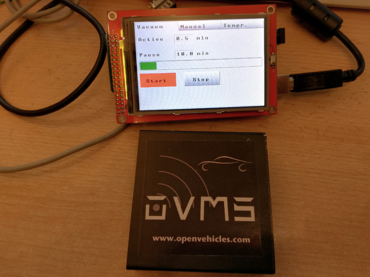
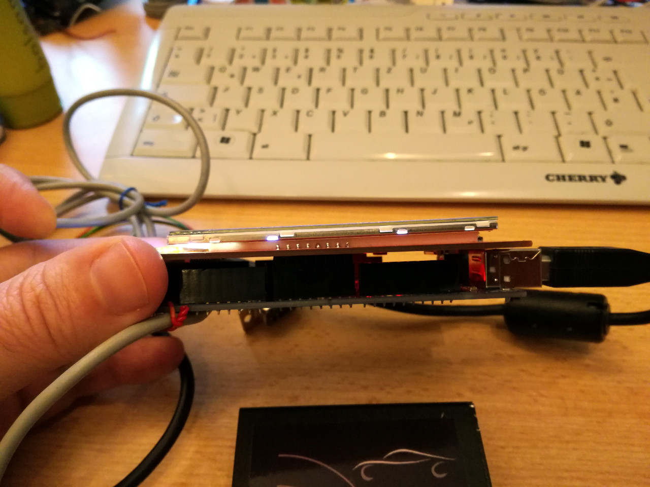
Here's a 3.5 inch TFT touch screen for Arduino compared to the V2 box. It's this one: http://hobbycomponents.com/shields/642-mcu-friend-35-colour-tft-touch-screen The TFT module itself is just 3mm thick: This kind of display would already make a great dashboard addition. But we should select one with a proper touch layer adjustment, this one from mcufriend has blind areas at two screen edges (calibration won't help with that). Regards, Michael Am 19.05.2017 um 16:40 schrieb Mark Webb-Johnson:
I see what you are saying. Using a raspberry pi with a 3.5" display as an example, that doesn't fit at all on the old OVMS v2 case, but would fit on our side-by-side option (A) board.
In fact, the Raspberry pi style cases are a pretty good size. A bit bigger than OVMS v2, but still reasonable. For example, the case below is 4" x 2.8" x 1.25" (deep). 100mm x 70mm x 30mm. That is a pretty nice size. Those 3.5" SPI touch panel displays are about U$10 for quantity 1.
I wonder if we could squeeze this down to something exactly the same size as a raspberry pi? With the same mounting holes. There are a lot of cases around for that, and many 3D printing templates for something to be customized. The width is about right, but we would have to go to a stacked arrangement. Something big enough for a 3.5" display.
Mark
On 19 May 2017, at 8:56 PM, Michael Balzer <dexter@expeedo.de> wrote:
That looks great :)
From a first test (A) should still fit in the Twizy glove box, so should fit in other mounting places as well.
As mentioned earlier I think a touch screen would make a nice addon, and (A) seems to be better for mounting a large display directly to the board. That should still make a nice & handy box.
I think (B) would become very clunky with a large display.
So I'm tending towards (A).
Regards, Michael
Am 19.05.2017 um 08:23 schrieb Mark Webb-Johnson: But, having seen it and held it, I'm now having second thoughts about the layout. As you can see from the attached pictures, the expansion slots are each about 60mm x 45mm. Putting two of those on the board makes it about 9.5cm x 9.5cm square. Height will be similar (a little bit taller) than the current OVMS v2. This is a first draft run only, just to confirm the components, but as you can see there is quite a lot of blank space and traces for the two expansion slots. That, and the sheer number of connectors we have, dominate the board. Let's call this arrangement (A).
There was an alternative arrangement that I considered a while back. That would be to have just one expansion slot, but use stackable connectors (so multiple boards could be piggybacked on each other). In that arrangement, the expansion slot could be either vertical or horizontal, with a vertical arrangement being close in size to the existing OVMS v2 (but the height would need to be much taller to accommodate the piggybacked expansion boards). Let's call this arrangement (B).
It doesn't change the wiring. Just the size and arrangement of components on the board, as well as the box housing this all. (A) ends up with a 1" wider+taller box of about the same thickness, while (B) ends up with a box about the same width and height, but significantly thicker. To me, it seems that (A) is more automotive, and (B) more hobbyist.
What do people think?
-- Michael Balzer * Helkenberger Weg 9 * D-58256 Ennepetal Fon 02333 / 833 5735 * Handy 0176 / 206 989 26
_______________________________________________ OvmsDev mailing list OvmsDev@lists.teslaclub.hk http://lists.teslaclub.hk/mailman/listinfo/ovmsdev
_______________________________________________ OvmsDev mailing list OvmsDev@lists.teslaclub.hk http://lists.teslaclub.hk/mailman/listinfo/ovmsdev
-- Michael Balzer * Helkenberger Weg 9 * D-58256 Ennepetal Fon 02333 / 833 5735 * Handy 0176 / 206 989 26


What about iTead Nextion displays? Despite having to use a Windows app to design the interface (then update the display directly or with a file on an uSD for everyone else), the display itself uses plain light UART to communicate... The new ones have extra gpios and sound generation... Cheap enough, the only thing that bothers me is that they are closed source otherwise. JB -- Julien Banchet +33651886877 On 19 May 2017, 23:28 +0200, Greg D. <gregd2350@gmail.com>, wrote:
I'm using this one with my Raspberry Pi. http://www.mcmelectronics.com/product/83-16786 There's also a larger one. I have it mounted separate from the Pi itself, which is perhaps an issue (ugly cables), but the larger pixel count makes the full X environment usable. Resistive touch overlay seems to work well with a stylus / fingernail, where capacitive touch and finger is too sensitive in a bouncing car, and too imprecise for many apps..
Which leads me to a question: Architecturally, is it better to have the display hosted directly on the OVMS module, or to have it talk to an off-board server such as the Pi, or have both of them meet up somewhere in the Cloud?
Greg
P.s. Also another preference here for option (A). I think a thinner board will go better under the dash (glove box) of the Roadster, where a thicker box would extend down and perhaps be visible. But, I don't think it's a show-stopper either way.
Michael Balzer wrote:
Here's a 3.5 inch TFT touch screen for Arduino compared to the V2 box.
It's this one: http://hobbycomponents.com/shields/642-mcu-friend-35-colour-tft-touch-screen
The TFT module itself is just 3mm thick:
This kind of display would already make a great dashboard addition.
But we should select one with a proper touch layer adjustment, this one from mcufriend has blind areas at two screen edges (calibration won't help with that).
Regards, Michael
Am 19.05.2017 um 16:40 schrieb Mark Webb-Johnson:
I see what you are saying. Using a raspberry pi with a 3.5" display as an example, that doesn't fit at all on the old OVMS v2 case, but would fit on our side-by-side option (A) board. In fact, the Raspberry pi style cases are a pretty good size. A bit bigger than OVMS v2, but still reasonable. For example, the case below is 4" x 2.8" x 1.25" (deep). 100mm x 70mm x 30mm. That is a pretty nice size. Those 3.5" SPI touch panel displays are about U$10 for quantity 1. I wonder if we could squeeze this down to something exactly the same size as a raspberry pi? With the same mounting holes. There are a lot of cases around for that, and many 3D printing templates for something to be customized. The width is about right, but we would have to go to a stacked arrangement. Something big enough for a 3.5" display. Mark On 19 May 2017, at 8:56 PM, Michael Balzer <dexter@expeedo.de> (mailto:dexter@expeedo.de) wrote:
That looks great :) From a first test (A) should still fit in the Twizy glove box, so should fit in other mounting places as well. As mentioned earlier I think a touch screen would make a nice addon, and (A) seems to be better for mounting a large display directly to the board. That should still make a nice & handy box. I think (B) would become very clunky with a large display. So I'm tending towards (A). Regards, Michael
Am 19.05.2017 um 08:23 schrieb Mark Webb-Johnson: But, having seen it and held it, I'm now having second thoughts about the layout. As you can see from the attached pictures, the expansion slots are each about 60mm x 45mm. Putting two of those on the board makes it about 9.5cm x 9.5cm square. Height will be similar (a little bit taller) than the current OVMS v2. This is a first draft run only, just to confirm the components, but as you can see there is quite a lot of blank space and traces for the two expansion slots. That, and the sheer number of connectors we have, dominate the board. Let's call this arrangement (A). There was an alternative arrangement that I considered a while back. That would be to have just one expansion slot, but use stackable connectors (so multiple boards could be piggybacked on each other). In that arrangement, the expansion slot could be either vertical or horizontal, with a vertical arrangement being close in size to the existing OVMS v2 (but th e height would need to be much taller to accommodate the piggybacked expansion boards). Let's call this arrangement (B). It doesn't change the wiring. Just the size and arrangement of components on the board, as well as the box housing this all. (A) ends up with a 1" wider+taller box of about the same thickness, while (B) ends up with a box about the same width and height, but significantly thicker. To me, it seems that (A) is more automotive, and (B) more hobbyist. What do people think?
-- Michael Balzer * Helkenberger Weg 9 * D-58256 Ennepetal Fon 02333 / 833 5735 (tel:02333%20/%20833%205735) * Handy 0176 / 206 989 26 (tel:0176%20/%20206%20989%2026) _______________________________________________ OvmsDev mailing list OvmsDev@lists.teslaclub.hk (mailto:OvmsDev@lists.teslaclub.hk) http://lists.teslaclub.hk/mailman/listinfo/ovmsdev
_______________________________________________ OvmsDev mailing list OvmsDev@lists.teslaclub.hk (mailto:OvmsDev@lists.teslaclub.hk) http://lists.teslaclub.hk/mailman/listinfo/ovmsdev -- Michael Balzer * Helkenberger Weg 9 * D-58256 Ennepetal Fon 02333 / 833 5735 (tel:02333%20/%20833%205735) * Handy 0176 / 206 989 26 (tel:0176%20/%20206%20989%2026)
_______________________________________________ OvmsDev mailing list OvmsDev@lists.teslaclub.hk (mailto:OvmsDev@lists.teslaclub.hk) http://lists.teslaclub.hk/mailman/listinfo/ovmsdev
OvmsDev mailing list OvmsDev@lists.teslaclub.hk http://lists.teslaclub.hk/mailman/listinfo/ovmsdev

Mark, My particular OVMS application is the Tesla Roadster. I have the v1 module installed against the "firewall" above the center console. It barely fits there because of the antenna connector extending on the long side. The vertical space available is just 10cm. The (A) layout would likely exceed that dimension once it's in a box, so I prefer the (B) layout. Perhaps the concern about height with the (B) layout could be mitigated by having two box choices accommodating one or two daughter boards. The size of the Raspberry Pi would be OK, but existing boxes would not likely be suitable because they would probably have holes cut to fit the connectors on the Pi. -- Steve

I'm a bit of an odd customer. I have both the V1 and V2, but have never activated a SIM for either of them. My interest is in discovering what is on the CAN bus, and having a familiar programming platform like the PIC as a way to investigate. I'm perfectly willing to use on-board storage and read out the data manually rather than hassle with activation, accounts, and periodic payments. For me, the main advantage of the V3 is the second CAN bus. I imagine that adding a second CAN connector necessarily makes the V3 larger than the V1 & V2, but it's worth it for that feature. I'm personally less interested in having two expansion boards, especially if the second expansion makes the case significantly larger than it would be just for the second CAN bus connector. Then again, I may be the only customer not interested in the SIM communications abilities. If I ever get a stable firmware and stop investigating, then I probably would jump on a SIM and enable remote data gathering. My application is the Tesla Roadster, so I have similar size constraints as Stephen and others. Brian p.s. The upgrade from PIC to ARM is a welcome advantage. I'm familiar enough with PIC to not count that processor as much of a negative, but ARM is a solid positive feature. I'm currently working on a Texas Instruments (Stellaris) Cortex-M4 for another design project. On May 18, 2017, at 11:23 PM, Mark Webb-Johnson <mark@webb-johnson.net> wrote:
I've got the first OVMS v3 development board in my hands now. The components seem fine, and I'm finalizing the QC program that checks everything to make sure all is ok. 16MB flash with OTA capability, Wifi, Bluetooth, 3xCAN bus, lots of GPIO, switched 12V, power by USB/12V, SD card reader/writer, optional 2G/3G/4G modem (with GPS), two expansion slots, USB, and an external expansion connector - all look good.
Both 3G and 4G development expansion boards are also being made now, and I should have those next week.
But, having seen it and held it, I'm now having second thoughts about the layout. As you can see from the attached pictures, the expansion slots are each about 60mm x 45mm. Putting two of those on the board makes it about 9.5cm x 9.5cm square. Height will be similar (a little bit taller) than the current OVMS v2. This is a first draft run only, just to confirm the components, but as you can see there is quite a lot of blank space and traces for the two expansion slots. That, and the sheer number of connectors we have, dominate the board. Let's call this arrangement (A).
There was an alternative arrangement that I considered a while back. That would be to have just one expansion slot, but use stackable connectors (so multiple boards could be piggybacked on each other). In that arrangement, the expansion slot could be either vertical or horizontal, with a vertical arrangement being close in size to the existing OVMS v2 (but the height would need to be much taller to accommodate the piggybacked expansion boards). Let's call this arrangement (B).
It doesn't change the wiring. Just the size and arrangement of components on the board, as well as the box housing this all. (A) ends up with a 1" wider+taller box of about the same thickness, while (B) ends up with a box about the same width and height, but significantly thicker. To me, it seems that (A) is more automotive, and (B) more hobbyist.
What do people think?
In the meantime, on with development (now that at last I have a target in my hands).
Mark
I'm still trying to work out the stackable/side-by-side issue. The thing I didn't like with the stackable option is the height (assuming each expansion module is also stackable). Every time I look at Arduino / Raspberry / etc, I think it is too tall. My problem is that top-most stackable connector that is _always_ empty. I know why it is there - but it just increases the height for the enclosure. I am thinking that perhaps there is a way out. What if we used a stackable design, but just have the modem modules non-stackable? The modem always goes on top. That way, the height of a normal system (without expansion modules other than the modem) is mostly unaffected. If an expansion module is required, then it must be stackable and placed between the main board and the modem. The non-stackable modem always on top. So for the 5% of users who use in-the-box expansion, they need a bigger case, but the 95% of other users can go with something slimmer. Kind of like this: Base board on the bottom, stackable expansion boards in the middle, and non-stackable modem board on top. The top picture shows the 5% case (with stackable expansion module sandwiched), the bottom picture shows the 95% case (with just base and modem). Size wise, we could go with something more like an Aurduido Due. Wider than OVMS v2, but about the same height and depth. Thoughts? Regards, Mark.
On 19 May 2017, at 2:23 PM, Mark Webb-Johnson <mark@webb-johnson.net> wrote:
I've got the first OVMS v3 development board in my hands now. The components seem fine, and I'm finalizing the QC program that checks everything to make sure all is ok. 16MB flash with OTA capability, Wifi, Bluetooth, 3xCAN bus, lots of GPIO, switched 12V, power by USB/12V, SD card reader/writer, optional 2G/3G/4G modem (with GPS), two expansion slots, USB, and an external expansion connector - all look good.
Both 3G and 4G development expansion boards are also being made now, and I should have those next week.
But, having seen it and held it, I'm now having second thoughts about the layout. As you can see from the attached pictures, the expansion slots are each about 60mm x 45mm. Putting two of those on the board makes it about 9.5cm x 9.5cm square. Height will be similar (a little bit taller) than the current OVMS v2. This is a first draft run only, just to confirm the components, but as you can see there is quite a lot of blank space and traces for the two expansion slots. That, and the sheer number of connectors we have, dominate the board. Let's call this arrangement (A).
There was an alternative arrangement that I considered a while back. That would be to have just one expansion slot, but use stackable connectors (so multiple boards could be piggybacked on each other). In that arrangement, the expansion slot could be either vertical or horizontal, with a vertical arrangement being close in size to the existing OVMS v2 (but the height would need to be much taller to accommodate the piggybacked expansion boards). Let's call this arrangement (B).
It doesn't change the wiring. Just the size and arrangement of components on the board, as well as the box housing this all. (A) ends up with a 1" wider+taller box of about the same thickness, while (B) ends up with a box about the same width and height, but significantly thicker. To me, it seems that (A) is more automotive, and (B) more hobbyist.
What do people think?
In the meantime, on with development (now that at last I have a target in my hands).
Mark
<image1.jpeg>
<image2.jpeg>
<image3.jpeg>
<image4.jpeg>
<image5.jpeg>
<image6.jpeg>
<image7.jpeg> _______________________________________________ OvmsDev mailing list OvmsDev@lists.teslaclub.hk http://lists.teslaclub.hk/mailman/listinfo/ovmsdev
On Mon, 22 May 2017, Mark Webb-Johnson wrote:
What if we used a stackable design, but just have the modem modules non-stackable? The modem always goes on top. That way, the height of a normal system (without expansion modules other than the modem) is mostly unaffected. If an expansion module is required, then it must be stackable and placed between the main board and the modem. The non-stackable modem always on top. So for the 5% of users who use in-the-box expansion, they need a bigger case, but the 95% of other users can go with something slimmer.
Sounds good to me. -- Steve
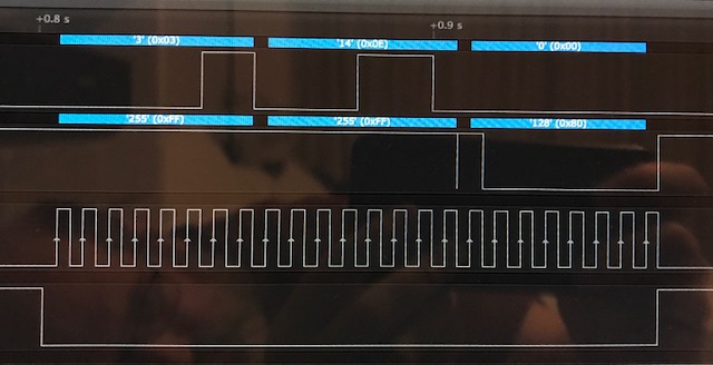
Just a short update on progress. It was painful, but we’ve finished the validation of the OVMS v3 board. Only one ESP32 was blown in the entire testing process ;-) [ Putting a 12V pin just next to a 3.3V pin on the switched 12V probably wasn’t such a smart idea. ] Oh well, at least I had fun with a microscope and some SMT soldering skills. Some nasty bugs and documentation issues on the ESP32 side of things, as well as an inadvertently swapped pair of MOSI / MISO pins caused endless issues. Thank Saleae for logic analysers. Really rather cool to watch the logic analyser display SPI bus traffic to/from the MCP2515, then CAN bus output of the message itself. Most of the issues we’ve been having are because the ESP32 internal pull-up system just doesn’t seem to be working well. Some of the GPIO pins have to use the RTC side to do pull-up, and behave the worst. We often get 2.1V, not 3.3V, measured; and it just doesn’t seem reliable (especially on the high speed side such as SPI and SD-card access). Switching to physical pull-ups resolve these issues, so that is what we are doing. There were also issues with dual-purposes GPIO lines used during bootstrapping. For example, the GPIO2 line (which must be low during boot for firmware download), and GPIO12 (which is used during boot for 1.8v / 3.3v flash selection). We’re also going to prepare pull-up pads for the other lines, and some test clip connection points, but leave them unpopulated - should be easier to change things in future, if necessary. To keep the high-speed SPI buses used to talk to the MCP2515 and MAX7317 short and clean, we’ve had to remove those three pins from the DB26 external expansion connector. It just seemed to be causing too much interference. These pins are still available on the expansion slot(s), and the SPI master driver we have switched to supports software control of the CS lines, so can support more than 3 SPI slaves on one master. Here is the current status: Power supply: vehicle 12V 3.3V: 3.300V measured and very stable - pass EXT_PWR: 11.704V measured - pass EXT_12V: 12.002V measured - pass USB_5V: 0.7013V measured (floating?) - pass Power supply: USB 5V 3.3V: 3.301V measured and very stable - pass EXT_PWR: 4.525V measured - pass EXT_12V: 0.0012V measured - pass USB_5V: 4.810V measured - pass Power supply: vehicle 12V and USB 5V 3.3V: 3.301V measured and very stable - pass EXT_PWR: 11.771V measured - pass EXT_12V: 12.031V measured - pass USB_5V: 4.838V measured - pass Reset Button Tested ok - pass Boot Button Tested ok - pass CP2102 Async comms: Tested ok - pass Automatic firmware download: Tested ok - pass Wifi Tested ok - pass Bluetooth Tested ok - pass External flash Special ESP32 fuse settings required Tested ok - pass SD-CARD 1-line mode: physical pull-ups added - pass 10K pull-up needed on GPIO14, GPIO15, GPIO4, GPIO13 Link required between GPIO0 and GPIO2 Special pull up and fuse setting arrangement needed for GPIO12 4-line mode: physical pull-ups added - pass 10K pull-up needed on GPIO14, GPIO15, GPIO4, GPIO13 Link required between GPIO0 and GPIO2 Special pull up and fuse setting arrangement needed for GPIO12 ESP32 CAN bus #0 - pass 1MHz bus speed Transmit: Working perfectly - pass Receive: Working perfectly - pass MCP2515 CAN bus #1 SPI MOSI/MISO swapped 1MHz bus speed Transmit: Working perfectly - pass Receive: Working perfectly - pass MCP2515 CAN bus #2 SPI MOSI/MISO swapped 1MHz bus speed Transmit: Working perfectly - pass Receive: Working perfectly - pass MAX7317 Remove pull-down to GND on SW_CTL, and add physical pull-up. Add pull-up on SP_CS3. Tested, and works ok - pass Vehicle 9 pin port Visually ok - pass Connections ok Expansion 26 pin port Visually ok - pass SPI MOSI/MISO swapped Connections ok USB port Visually ok - pass To change to a physically stronger port (or mounting arrangement) Expansion slot #1 Visually ok - pass Expansion slot #2 Visually ok - pass To be removed in production board Burning the ESP32 fuses was exciting. This is a one-time operation with no way back. It is literally passing too much current through some little wires in the chip, to burn through and break the wire. Blowing the fuse. Once we do it, here is what we get: $ espefuse.py -p /dev/tty.SLAB_USBtoUART burn_efuse XPD_SDIO_REG 1 $ espefuse.py -p /dev/tty.SLAB_USBtoUART burn_efuse XPD_SDIO_TIEH 1 $ espefuse.py -p /dev/tty.SLAB_USBtoUART burn_efuse XPD_SDIO_FORCE 1 $ espefuse.py -p /dev/tty.SLAB_USBtoUART burn_efuse SPI_PAD_CONFIG_CLK 6 $ espefuse.py -p /dev/tty.SLAB_USBtoUART burn_efuse SPI_PAD_CONFIG_Q 7 $ espefuse.py -p /dev/tty.SLAB_USBtoUART burn_efuse SPI_PAD_CONFIG_D 8 $ espefuse.py -p /dev/tty.SLAB_USBtoUART burn_efuse SPI_PAD_CONFIG_HD 9 $ espefuse.py -p /dev/tty.SLAB_USBtoUART burn_efuse SPI_PAD_CONFIG_CS0 22 $ espefuse.py -p /dev/tty.SLAB_USBtoUART summary XPD_SDIO_FORCE Ignore MTDI pin (GPIO12) for VDD_SDIO on reset = 1 R/W (0x1) XPD_SDIO_REG If XPD_SDIO_FORCE, enable VDD_SDIO reg on reset = 1 R/W (0x1) XPD_SDIO_TIEH If XPD_SDIO_FORCE & XPD_SDIO_REG, 1=3.3V 0=1.8V = 1 R/W (0x1) SPI_PAD_CONFIG_CLK Override SD_CLK pad (GPIO6/SPICLK) = 6 R/W (0x6) SPI_PAD_CONFIG_Q Override SD_DATA_0 pad (GPIO7/SPIQ) = 7 R/W (0x7) SPI_PAD_CONFIG_D Override SD_DATA_1 pad (GPIO8/SPID) = 8 R/W (0x8) SPI_PAD_CONFIG_HD Override SD_DATA_2 pad (GPIO9/SPIHD) = 9 R/W (0x9) SPI_PAD_CONFIG_CS0 Override SD_CMD pad (GPIO11/SPICS0) = 22 R/W (0x16) Once that is done, we can simply change to DIO mode for SPI flashing and set flash size to 16MB - it will now use our external 16MB flash and the WROOM-32 4MB flash will not be used. In theory, we should still be able access the WROOM-32 4MB flash in our code, but it is not used by the system. This procedure will be done by the factory, as part of factory firmware load. So, yesterday I handed the final list of all the above over to the China guys. We’re happy that the board is close enough to try to make a production version, so they are sourcing an enclosure and re-laying everything out to fit and match that. The goal is to get the system about the same height and depth as an OVMS v2 module, just about an inch longer. Biggest constraint seems to be the number and size of external connectors we have. Here is what I sent China: and this is what they sent back: Touché, China. You win that one. We’re trying to find some low-profile stacking connectors to keep the depth reasonable. So, the enclosure selection and final board layout is being drawn up now by the China side. I’m taking a break from banging on SPI buses, and now full-time on the firmware framework. Regards, Mark.
On 22 May 2017, at 10:58 AM, Mark Webb-Johnson <mark@webb-johnson.net> wrote:
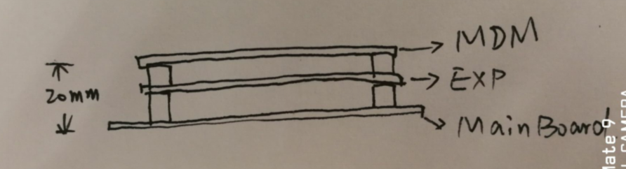
I'm still trying to work out the stackable/side-by-side issue.
The thing I didn't like with the stackable option is the height (assuming each expansion module is also stackable). Every time I look at Arduino / Raspberry / etc, I think it is too tall. My problem is that top-most stackable connector that is _always_ empty. I know why it is there - but it just increases the height for the enclosure.
I am thinking that perhaps there is a way out.
What if we used a stackable design, but just have the modem modules non-stackable? The modem always goes on top. That way, the height of a normal system (without expansion modules other than the modem) is mostly unaffected. If an expansion module is required, then it must be stackable and placed between the main board and the modem. The non-stackable modem always on top. So for the 5% of users who use in-the-box expansion, they need a bigger case, but the 95% of other users can go with something slimmer.
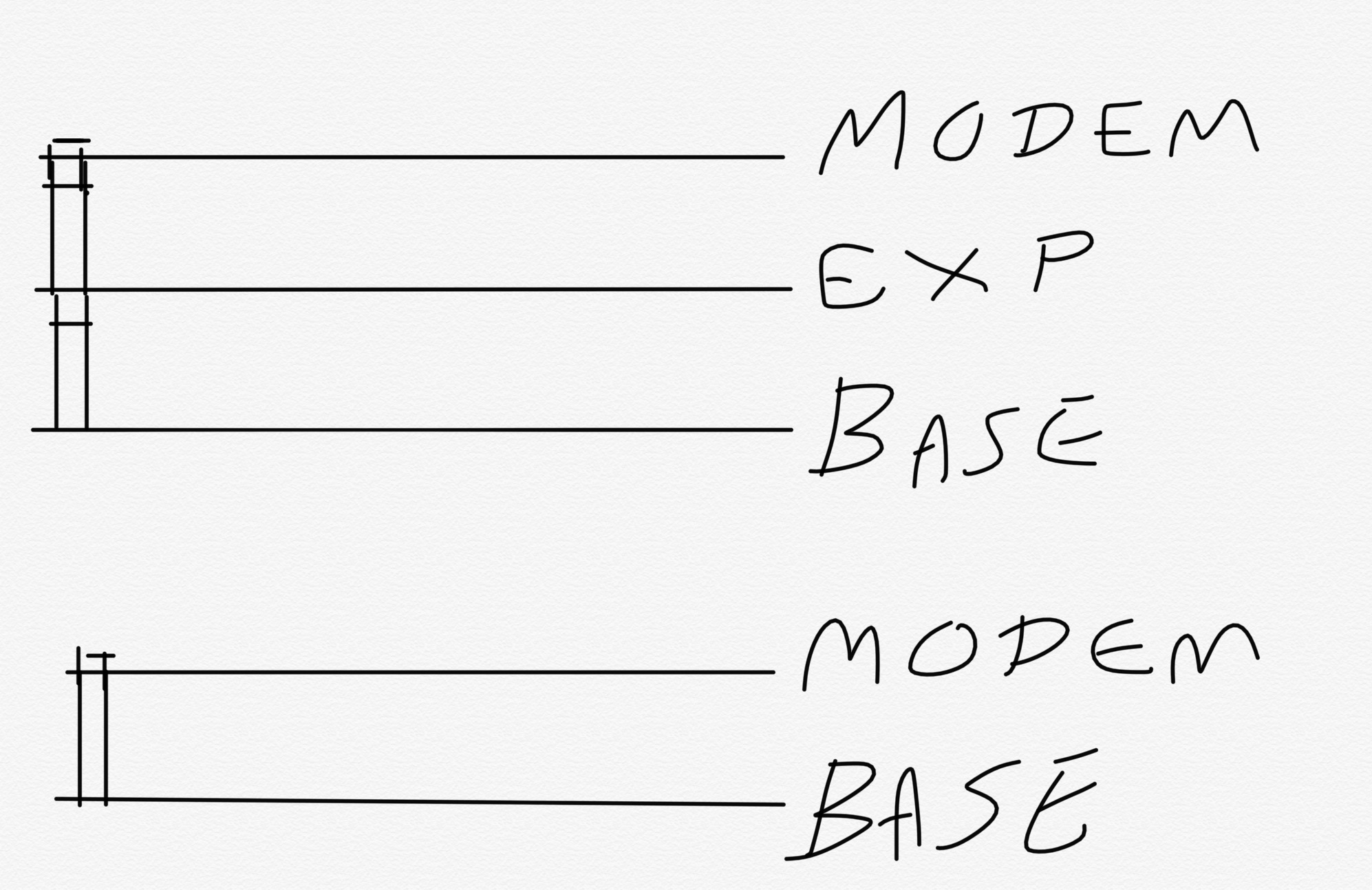
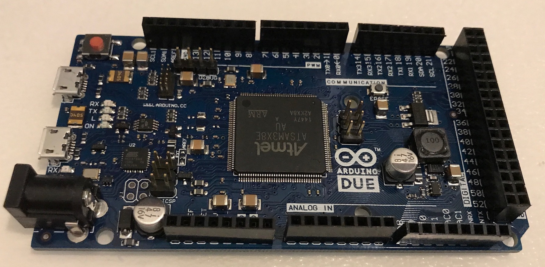
Kind of like this: Base board on the bottom, stackable expansion boards in the middle, and non-stackable modem board on top. The top picture shows the 5% case (with stackable expansion module sandwiched), the bottom picture shows the 95% case (with just base and modem).
Size wise, we could go with something more like an Aurduido Due. Wider than OVMS v2, but about the same height and depth.
Thoughts?
Regards, Mark.
<image1.jpeg>
<image2.jpeg>
On 19 May 2017, at 2:23 PM, Mark Webb-Johnson <mark@webb-johnson.net> wrote:
I've got the first OVMS v3 development board in my hands now. The components seem fine, and I'm finalizing the QC program that checks everything to make sure all is ok. 16MB flash with OTA capability, Wifi, Bluetooth, 3xCAN bus, lots of GPIO, switched 12V, power by USB/12V, SD card reader/writer, optional 2G/3G/4G modem (with GPS), two expansion slots, USB, and an external expansion connector - all look good.
Both 3G and 4G development expansion boards are also being made now, and I should have those next week.
But, having seen it and held it, I'm now having second thoughts about the layout. As you can see from the attached pictures, the expansion slots are each about 60mm x 45mm. Putting two of those on the board makes it about 9.5cm x 9.5cm square. Height will be similar (a little bit taller) than the current OVMS v2. This is a first draft run only, just to confirm the components, but as you can see there is quite a lot of blank space and traces for the two expansion slots. That, and the sheer number of connectors we have, dominate the board. Let's call this arrangement (A).
There was an alternative arrangement that I considered a while back. That would be to have just one expansion slot, but use stackable connectors (so multiple boards could be piggybacked on each other). In that arrangement, the expansion slot could be either vertical or horizontal, with a vertical arrangement being close in size to the existing OVMS v2 (but the height would need to be much taller to accommodate the piggybacked expansion boards). Let's call this arrangement (B).
It doesn't change the wiring. Just the size and arrangement of components on the board, as well as the box housing this all. (A) ends up with a 1" wider+taller box of about the same thickness, while (B) ends up with a box about the same width and height, but significantly thicker. To me, it seems that (A) is more automotive, and (B) more hobbyist.
What do people think?
In the meantime, on with development (now that at last I have a target in my hands).
Mark
<image1.jpeg>
<image2.jpeg>
<image3.jpeg>
<image4.jpeg>
<image5.jpeg>
<image6.jpeg>
<image7.jpeg> _______________________________________________ OvmsDev mailing list OvmsDev@lists.teslaclub.hk http://lists.teslaclub.hk/mailman/listinfo/ovmsdev
OvmsDev mailing list OvmsDev@lists.teslaclub.hk http://lists.teslaclub.hk/mailman/listinfo/ovmsdev
Am 09.06.2017 um 07:41 schrieb Mark Webb-Johnson:
Just a short update on progress.
...a Mark Webb-Johnson version of "short" :) Thanks for that insight into the hardware development process! I especially like all those green "pass" signals :) So we can now go straight forward to using production modules for the vehicle adaption? I hope there will be fewer bugs on the software side... Regards, Michael -- Michael Balzer * Helkenberger Weg 9 * D-58256 Ennepetal Fon 02333 / 833 5735 * Handy 0176 / 206 989 26
I didn't have time to write a short letter, so I wrote a long one instead. (famous quote attributed to Mark Twain)
I especially like all those green "pass" signals :)
There was a lot more red a week or so ago.
So we can now go straight forward to using production modules for the vehicle adaption?
Yep, that’s the idea now. We’ll probably make another couple of ‘final’ boards to make sure all is ok. Check those, and if no problems then hand make another twenty or so for developers. If no problems reported, then make a large first production batch. Getting close now.
I hope there will be fewer bugs on the software side…
At least those can be fixed by over-the-air software update. I’m more worried about the bugs that need a soldering iron to squash. Regards, Mark.
On 9 Jun 2017, at 3:02 PM, Michael Balzer <dexter@expeedo.de> wrote:
Am 09.06.2017 um 07:41 schrieb Mark Webb-Johnson:
Just a short update on progress.
...a Mark Webb-Johnson version of "short" :)
Thanks for that insight into the hardware development process!
I especially like all those green "pass" signals :)
So we can now go straight forward to using production modules for the vehicle adaption?
I hope there will be fewer bugs on the software side...
Regards, Michael
-- Michael Balzer * Helkenberger Weg 9 * D-58256 Ennepetal Fon 02333 / 833 5735 * Handy 0176 / 206 989 26
_______________________________________________ OvmsDev mailing list OvmsDev@lists.teslaclub.hk http://lists.teslaclub.hk/mailman/listinfo/ovmsdev

On 09/06/17 19:29, Mark Webb-Johnson wrote:
Yep, that’s the idea now. We’ll probably make another couple of ‘final’ boards to make sure all is ok. Check those, and if no problems then hand make another twenty or so for developers. If no problems reported, then make a large first production batch. Getting close now.
I would be keen to get a developer board. The Leaf has 3 CAN buses (CAR, EV and Chademo) on the OBD2 connector and I really want to get the odometer value which isn't available on the EV bus we're on at the moment. I've also discovered that the 2016 model moved the TCU to the CAR bus, which may mean that we cannot do remote climate control on the EV bus -- the old messages on the EV bus don't work, I haven't had a chance to try them on the CAR bus. Are you going to make new cables for the OBD2 port now or later? I can make one up for the Leaf and verify it works on all the buses. I haven't looked at what is on the Chademo bus, but watching the battery current and voltage reported on the EV bus as we currently do seems sufficient for knowing what is going on during DC Quick charging. Hence I feel we should supply a cable for the CAR and EV bus, leaving the 3rd bus for future expansion, for example to MitM a component by connecting it to the 3rd bus and having the OVMS gateway messages to the rest of the car, or the currently discussed OBD2 HUD or other dongle. Can anyone recommend a source of low profile OBD2 plugs or a low profile extension cord that includes all the pins? I have plugs that are too big for use while driving and low profile extension cords that don't pass through all the pins :(
I hope there will be fewer bugs on the software side…
At least those can be fixed by over-the-air software update. I’m more worried about the bugs that need a soldering iron to squash.
We'll have to think very carefully about security for the code upload -- being careful not to implement risky functionality is moot when you can upload new code. The PIC's Harvard architecture and out of heap stack also made it pretty safe in the face of memory corruption bugs. Is the esp32 a von Neumann architecture? Is the stack in the same address space as the rest of system ram? Can pages be marked read only or no execute?
Our current cables for Leaf have two can buses wired on them already, and both should work with OVMS v3. I’m happy to make different cables for vehicles, if necessary. It is not too hard to arrange it here - the only issue is minimum order quantity usually 100 pieces or so. Regarding the OTA update, yes it is scary. The ESP32 is standard ARM32 architecture. The OTA system is such that we have full control of the download and install of the firmware image. The 16MB flash is partitioned into three code areas (each 4MB in size) - factory, ota#1, and ota#2. The idea is the ‘factory’ contains the factory image. If you are running from ‘factory’ and do an OTA update, it goes to ota#1, then the system reboots and you are running in ‘ota#1’ now. Then, if you do another OTA update, that goes into ota#2, then the system reboots and you are running in ‘ota#2’ now. Next OTA update goes to ota#1. There is a consistency check system such that if the current OTA partition is corrupt, it goes back to factory. There are other ways of doing this, but that is the default approach. The initial approach I am working on is to pull the OTA update via HTTPS, and use SSL certificate verification to ensure we are pulling from the correct location. Code signing would also be good to have, but I haven’t done it in the first version. Regards, Mark.
On 11 Jun 2017, at 9:21 AM, Tom Parker <tom@carrott.org> wrote:
On 09/06/17 19:29, Mark Webb-Johnson wrote:
Yep, that’s the idea now. We’ll probably make another couple of ‘final’ boards to make sure all is ok. Check those, and if no problems then hand make another twenty or so for developers. If no problems reported, then make a large first production batch. Getting close now.
I would be keen to get a developer board.
The Leaf has 3 CAN buses (CAR, EV and Chademo) on the OBD2 connector and I really want to get the odometer value which isn't available on the EV bus we're on at the moment. I've also discovered that the 2016 model moved the TCU to the CAR bus, which may mean that we cannot do remote climate control on the EV bus -- the old messages on the EV bus don't work, I haven't had a chance to try them on the CAR bus.
Are you going to make new cables for the OBD2 port now or later? I can make one up for the Leaf and verify it works on all the buses. I haven't looked at what is on the Chademo bus, but watching the battery current and voltage reported on the EV bus as we currently do seems sufficient for knowing what is going on during DC Quick charging. Hence I feel we should supply a cable for the CAR and EV bus, leaving the 3rd bus for future expansion, for example to MitM a component by connecting it to the 3rd bus and having the OVMS gateway messages to the rest of the car, or the currently discussed OBD2 HUD or other dongle.
Can anyone recommend a source of low profile OBD2 plugs or a low profile extension cord that includes all the pins? I have plugs that are too big for use while driving and low profile extension cords that don't pass through all the pins :(
I hope there will be fewer bugs on the software side…
At least those can be fixed by over-the-air software update. I’m more worried about the bugs that need a soldering iron to squash.
We'll have to think very carefully about security for the code upload -- being careful not to implement risky functionality is moot when you can upload new code. The PIC's Harvard architecture and out of heap stack also made it pretty safe in the face of memory corruption bugs. Is the esp32 a von Neumann architecture? Is the stack in the same address space as the rest of system ram? Can pages be marked read only or no execute? _______________________________________________ OvmsDev mailing list OvmsDev@lists.teslaclub.hk http://lists.teslaclub.hk/mailman/listinfo/ovmsdev
On Jun 8, 2017, at 10:41 PM, Mark Webb-Johnson <mark@webb-johnson.net> wrote:
Really rather cool to watch the logic analyser display SPI bus traffic to/from the MCP2515, then CAN bus output of the message itself.
It's all about the protocol analyzer. They can be expensive for full-sized oscilloscopes. I used a Tektronix with I2S and I8S decoding on a system with 32 audio channels on 4 data lines (8 channels per serial data line), and the 'scope displayed the audio samples as hex values right on the LCD. Does the Saleae software product actually decode CAN protocol? On Jun 10, 2017, at 6:21 PM, Tom Parker <tom@carrott.org> wrote:
We'll have to think very carefully about security for the code upload -- being careful not to implement risky functionality is moot when you can upload new code. The PIC's Harvard architecture and out of heap stack also made it pretty safe in the face of memory corruption bugs. Is the esp32 a von Neumann architecture? Is the stack in the same address space as the rest of system ram? Can pages be marked read only or no execute?
I'm not sure that I understand you perfectly, but I thought it might be interesting to point out that the older Microchip compiler did not use the hardware (15-level) stack. Instead, the old C compiler implemented a software virtual stack using one of the three pseudo address pointer registers in the PIC18. The old way meant that C code operated pretty much the same as it would on "normal" processors, albeit a few cycles slower per push/pop operation. When Microchip purchased the High Tech C compiler (at least I think that's the one they bought), this switched over to using the limited hardware stack for function return addresses only, combined with code analysis to detect call trees that might be too deep for the limited stack as well as placing automatic variables that would be on the stack into fixed RAM addresses. They even go so far as to treat interrupt call trees separately from the main, allocating two versions of automatic variables to simulate the way they would be separate if they'd been allocated on the stack. This is a great optimization, but I ran into serious issues porting old C source written and tested on the Microchip compiler to the High Tech C compiler. I also believe that I found some serious bugs in the analyzer, but those all seem to be gone, now. As you might guess, I have a love/hate relationship with the PIC architecture. Brian Willoughby
The Saleae software is pretty cool. It supports SPI, CAN, etc. Full list of protocols is: SPI, I2C, serial, 1-Wire, CAN, UNI/O, I2S/PCM, MP Mode, Manchester, Modbus, DMX-512, Parallel, JTAG, LIN, Atmel SWI, MDIO, SWD, LCD HD44780, BiSS C, HDLC, HDMI CEC, PS/2, USB 1.1, Midi Triggering is the only let-down - it is pretty basic and just on level transitions. I use a US$10 clone with 8 channels and sampling up to 24million samples /sec. I really should buy something better, but that works great for me on the relatively low-speed embedded protocols. 1MHz stuff like CAN is no problem. I’ve also messed around with Sigrok <https://sigrok.org/>, which is pretty cool and supports the Saleae analyser clones. Regards, Mark.
On 11 Jun 2017, at 10:23 AM, HONDA S-2000 <s2000@audiobanshee.com> wrote:
On Jun 8, 2017, at 10:41 PM, Mark Webb-Johnson <mark@webb-johnson.net> wrote:
Really rather cool to watch the logic analyser display SPI bus traffic to/from the MCP2515, then CAN bus output of the message itself.
It's all about the protocol analyzer. They can be expensive for full-sized oscilloscopes. I used a Tektronix with I2S and I8S decoding on a system with 32 audio channels on 4 data lines (8 channels per serial data line), and the 'scope displayed the audio samples as hex values right on the LCD.
Does the Saleae software product actually decode CAN protocol?
On Jun 10, 2017, at 6:21 PM, Tom Parker <tom@carrott.org> wrote:
We'll have to think very carefully about security for the code upload -- being careful not to implement risky functionality is moot when you can upload new code. The PIC's Harvard architecture and out of heap stack also made it pretty safe in the face of memory corruption bugs. Is the esp32 a von Neumann architecture? Is the stack in the same address space as the rest of system ram? Can pages be marked read only or no execute?
I'm not sure that I understand you perfectly, but I thought it might be interesting to point out that the older Microchip compiler did not use the hardware (15-level) stack. Instead, the old C compiler implemented a software virtual stack using one of the three pseudo address pointer registers in the PIC18. The old way meant that C code operated pretty much the same as it would on "normal" processors, albeit a few cycles slower per push/pop operation.
When Microchip purchased the High Tech C compiler (at least I think that's the one they bought), this switched over to using the limited hardware stack for function return addresses only, combined with code analysis to detect call trees that might be too deep for the limited stack as well as placing automatic variables that would be on the stack into fixed RAM addresses. They even go so far as to treat interrupt call trees separately from the main, allocating two versions of automatic variables to simulate the way they would be separate if they'd been allocated on the stack. This is a great optimization, but I ran into serious issues porting old C source written and tested on the Microchip compiler to the High Tech C compiler. I also believe that I found some serious bugs in the analyzer, but those all seem to be gone, now.
As you might guess, I have a love/hate relationship with the PIC architecture.
Brian Willoughby
_______________________________________________ OvmsDev mailing list OvmsDev@lists.teslaclub.hk http://lists.teslaclub.hk/mailman/listinfo/ovmsdev
And we inch closer to the finishing line… Here’s the PCB layout (with copper layer removed to make it easier to see both sides). About the same height as OVMS v3, but an inch or so wider. I’ve also attached schematic, and top+bottom layer detail for the main as well as modem board. We’re trying to go with one modem board PCB, with different components put on it depending on 3G/4G modem. This _should_ be the final layout and arrangement made to fit the enclosure. We have two enclosure candidates: Metal shell, like ovms v2. If we use this, we need to bring out bluetooth/wifi antenna as well (to a little stubby antenna on the enclosure directly). Plastic shell, injection moulded. My preference is for #2, but I’m waiting to see it. The up-front cost for the injection moulding is high, but long-term is cheaper. We’re 3D printing a prototype at the moment (to get the design 100% before making the mould - to keep costs down). Firmware framework is progressing. Fighting missing bits in ESP32 newlib… #notquitethefulllibc Regards, Mark.
On 9 Jun 2017, at 1:41 PM, Mark Webb-Johnson <mark@webb-johnson.net> wrote:
Just a short update on progress.
It was painful, but we’ve finished the validation of the OVMS v3 board. Only one ESP32 was blown in the entire testing process ;-) [ Putting a 12V pin just next to a 3.3V pin on the switched 12V probably wasn’t such a smart idea. ] Oh well, at least I had fun with a microscope and some SMT soldering skills.
Some nasty bugs and documentation issues on the ESP32 side of things, as well as an inadvertently swapped pair of MOSI / MISO pins caused endless issues. Thank Saleae for logic analysers.
<image2.jpeg>
Really rather cool to watch the logic analyser display SPI bus traffic to/from the MCP2515, then CAN bus output of the message itself.
Most of the issues we’ve been having are because the ESP32 internal pull-up system just doesn’t seem to be working well. Some of the GPIO pins have to use the RTC side to do pull-up, and behave the worst. We often get 2.1V, not 3.3V, measured; and it just doesn’t seem reliable (especially on the high speed side such as SPI and SD-card access). Switching to physical pull-ups resolve these issues, so that is what we are doing. There were also issues with dual-purposes GPIO lines used during bootstrapping. For example, the GPIO2 line (which must be low during boot for firmware download), and GPIO12 (which is used during boot for 1.8v / 3.3v flash selection). We’re also going to prepare pull-up pads for the other lines, and some test clip connection points, but leave them unpopulated - should be easier to change things in future, if necessary.
To keep the high-speed SPI buses used to talk to the MCP2515 and MAX7317 short and clean, we’ve had to remove those three pins from the DB26 external expansion connector. It just seemed to be causing too much interference. These pins are still available on the expansion slot(s), and the SPI master driver we have switched to supports software control of the CS lines, so can support more than 3 SPI slaves on one master.
Here is the current status:
Power supply: vehicle 12V 3.3V: 3.300V measured and very stable - pass EXT_PWR: 11.704V measured - pass EXT_12V: 12.002V measured - pass USB_5V: 0.7013V measured (floating?) - pass Power supply: USB 5V 3.3V: 3.301V measured and very stable - pass EXT_PWR: 4.525V measured - pass EXT_12V: 0.0012V measured - pass USB_5V: 4.810V measured - pass Power supply: vehicle 12V and USB 5V 3.3V: 3.301V measured and very stable - pass EXT_PWR: 11.771V measured - pass EXT_12V: 12.031V measured - pass USB_5V: 4.838V measured - pass Reset Button Tested ok - pass Boot Button Tested ok - pass CP2102 Async comms: Tested ok - pass Automatic firmware download: Tested ok - pass Wifi Tested ok - pass Bluetooth Tested ok - pass External flash Special ESP32 fuse settings required Tested ok - pass SD-CARD 1-line mode: physical pull-ups added - pass 10K pull-up needed on GPIO14, GPIO15, GPIO4, GPIO13 Link required between GPIO0 and GPIO2 Special pull up and fuse setting arrangement needed for GPIO12 4-line mode: physical pull-ups added - pass 10K pull-up needed on GPIO14, GPIO15, GPIO4, GPIO13 Link required between GPIO0 and GPIO2 Special pull up and fuse setting arrangement needed for GPIO12 ESP32 CAN bus #0 - pass 1MHz bus speed Transmit: Working perfectly - pass Receive: Working perfectly - pass MCP2515 CAN bus #1 SPI MOSI/MISO swapped 1MHz bus speed Transmit: Working perfectly - pass Receive: Working perfectly - pass MCP2515 CAN bus #2 SPI MOSI/MISO swapped 1MHz bus speed Transmit: Working perfectly - pass Receive: Working perfectly - pass MAX7317 Remove pull-down to GND on SW_CTL, and add physical pull-up. Add pull-up on SP_CS3. Tested, and works ok - pass Vehicle 9 pin port Visually ok - pass Connections ok Expansion 26 pin port Visually ok - pass SPI MOSI/MISO swapped Connections ok USB port Visually ok - pass To change to a physically stronger port (or mounting arrangement) Expansion slot #1 Visually ok - pass Expansion slot #2 Visually ok - pass To be removed in production board
Burning the ESP32 fuses was exciting. This is a one-time operation with no way back. It is literally passing too much current through some little wires in the chip, to burn through and break the wire. Blowing the fuse. Once we do it, here is what we get:
$ espefuse.py -p /dev/tty.SLAB_USBtoUART burn_efuse XPD_SDIO_REG 1 $ espefuse.py -p /dev/tty.SLAB_USBtoUART burn_efuse XPD_SDIO_TIEH 1 $ espefuse.py -p /dev/tty.SLAB_USBtoUART burn_efuse XPD_SDIO_FORCE 1
$ espefuse.py -p /dev/tty.SLAB_USBtoUART burn_efuse SPI_PAD_CONFIG_CLK 6 $ espefuse.py -p /dev/tty.SLAB_USBtoUART burn_efuse SPI_PAD_CONFIG_Q 7 $ espefuse.py -p /dev/tty.SLAB_USBtoUART burn_efuse SPI_PAD_CONFIG_D 8 $ espefuse.py -p /dev/tty.SLAB_USBtoUART burn_efuse SPI_PAD_CONFIG_HD 9 $ espefuse.py -p /dev/tty.SLAB_USBtoUART burn_efuse SPI_PAD_CONFIG_CS0 22
$ espefuse.py -p /dev/tty.SLAB_USBtoUART summary XPD_SDIO_FORCE Ignore MTDI pin (GPIO12) for VDD_SDIO on reset = 1 R/W (0x1) XPD_SDIO_REG If XPD_SDIO_FORCE, enable VDD_SDIO reg on reset = 1 R/W (0x1) XPD_SDIO_TIEH If XPD_SDIO_FORCE & XPD_SDIO_REG, 1=3.3V 0=1.8V = 1 R/W (0x1)
SPI_PAD_CONFIG_CLK Override SD_CLK pad (GPIO6/SPICLK) = 6 R/W (0x6) SPI_PAD_CONFIG_Q Override SD_DATA_0 pad (GPIO7/SPIQ) = 7 R/W (0x7) SPI_PAD_CONFIG_D Override SD_DATA_1 pad (GPIO8/SPID) = 8 R/W (0x8) SPI_PAD_CONFIG_HD Override SD_DATA_2 pad (GPIO9/SPIHD) = 9 R/W (0x9) SPI_PAD_CONFIG_CS0 Override SD_CMD pad (GPIO11/SPICS0) = 22 R/W (0x16)
Once that is done, we can simply change to DIO mode for SPI flashing and set flash size to 16MB - it will now use our external 16MB flash and the WROOM-32 4MB flash will not be used. In theory, we should still be able access the WROOM-32 4MB flash in our code, but it is not used by the system. This procedure will be done by the factory, as part of factory firmware load.
So, yesterday I handed the final list of all the above over to the China guys. We’re happy that the board is close enough to try to make a production version, so they are sourcing an enclosure and re-laying everything out to fit and match that. The goal is to get the system about the same height and depth as an OVMS v2 module, just about an inch longer. Biggest constraint seems to be the number and size of external connectors we have.
Here is what I sent China:
<PastedGraphic-1.tiff>
and this is what they sent back:
<269B1E05-5609-4430-B04B-23D2A314D01E.png>
Touché, China. You win that one.
<6DBB6579-A139-46BE-8664-2C3B3D74C467.png>
We’re trying to find some low-profile stacking connectors to keep the depth reasonable.
So, the enclosure selection and final board layout is being drawn up now by the China side. I’m taking a break from banging on SPI buses, and now full-time on the firmware framework.
Regards, Mark.
On 22 May 2017, at 10:58 AM, Mark Webb-Johnson <mark@webb-johnson.net <mailto:mark@webb-johnson.net>> wrote:
I'm still trying to work out the stackable/side-by-side issue.
The thing I didn't like with the stackable option is the height (assuming each expansion module is also stackable). Every time I look at Arduino / Raspberry / etc, I think it is too tall. My problem is that top-most stackable connector that is _always_ empty. I know why it is there - but it just increases the height for the enclosure.
I am thinking that perhaps there is a way out.
What if we used a stackable design, but just have the modem modules non-stackable? The modem always goes on top. That way, the height of a normal system (without expansion modules other than the modem) is mostly unaffected. If an expansion module is required, then it must be stackable and placed between the main board and the modem. The non-stackable modem always on top. So for the 5% of users who use in-the-box expansion, they need a bigger case, but the 95% of other users can go with something slimmer.
Kind of like this: Base board on the bottom, stackable expansion boards in the middle, and non-stackable modem board on top. The top picture shows the 5% case (with stackable expansion module sandwiched), the bottom picture shows the 95% case (with just base and modem).
Size wise, we could go with something more like an Aurduido Due. Wider than OVMS v2, but about the same height and depth.
Thoughts?
Regards, Mark.
<image1.jpeg>
<image2.jpeg>
On 19 May 2017, at 2:23 PM, Mark Webb-Johnson <mark@webb-johnson.net <mailto:mark@webb-johnson.net>> wrote:
I've got the first OVMS v3 development board in my hands now. The components seem fine, and I'm finalizing the QC program that checks everything to make sure all is ok. 16MB flash with OTA capability, Wifi, Bluetooth, 3xCAN bus, lots of GPIO, switched 12V, power by USB/12V, SD card reader/writer, optional 2G/3G/4G modem (with GPS), two expansion slots, USB, and an external expansion connector - all look good.
Both 3G and 4G development expansion boards are also being made now, and I should have those next week.
But, having seen it and held it, I'm now having second thoughts about the layout. As you can see from the attached pictures, the expansion slots are each about 60mm x 45mm. Putting two of those on the board makes it about 9.5cm x 9.5cm square. Height will be similar (a little bit taller) than the current OVMS v2. This is a first draft run only, just to confirm the components, but as you can see there is quite a lot of blank space and traces for the two expansion slots. That, and the sheer number of connectors we have, dominate the board. Let's call this arrangement (A).
There was an alternative arrangement that I considered a while back. That would be to have just one expansion slot, but use stackable connectors (so multiple boards could be piggybacked on each other). In that arrangement, the expansion slot could be either vertical or horizontal, with a vertical arrangement being close in size to the existing OVMS v2 (but the height would need to be much taller to accommodate the piggybacked expansion boards). Let's call this arrangement (B).
It doesn't change the wiring. Just the size and arrangement of components on the board, as well as the box housing this all. (A) ends up with a 1" wider+taller box of about the same thickness, while (B) ends up with a box about the same width and height, but significantly thicker. To me, it seems that (A) is more automotive, and (B) more hobbyist.
What do people think?
In the meantime, on with development (now that at last I have a target in my hands).
Mark
<image1.jpeg>
<image2.jpeg>
<image3.jpeg>
<image4.jpeg>
<image5.jpeg>
<image6.jpeg>
<image7.jpeg> _______________________________________________ OvmsDev mailing list OvmsDev@lists.teslaclub.hk <mailto:OvmsDev@lists.teslaclub.hk> http://lists.teslaclub.hk/mailman/listinfo/ovmsdev
OvmsDev mailing list OvmsDev@lists.teslaclub.hk <mailto:OvmsDev@lists.teslaclub.hk> http://lists.teslaclub.hk/mailman/listinfo/ovmsdev
_______________________________________________ OvmsDev mailing list OvmsDev@lists.teslaclub.hk http://lists.teslaclub.hk/mailman/listinfo/ovmsdev
participants (10)
-
 Edward Cheeseman
 -
 Frank Demes
 -
 Greg D.
 -
 HONDA S-2000
 -
 Julien “JaXX” Banchet
 -
 Mark Webb-Johnson
 -
 Michael Balzer
 -
 Nikolay Shishkov
 -
 Stephen Casner
 -
 Tom Parker